Chitika
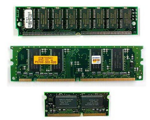
Computer Memory
This is implemented through the memory hierarchy of modern computers is based on two principles: the principle of locality of appeals and the ratio of price / performance. The principle of locality of references suggests that most programs do not fortunately appeals to all his commands and data with equal probability, and have a preference for a certain part of its address space.
Memory hierarchy of modern computers is based on several levels, with higher levels of smaller volume, faster and more cost per byte than the lower level. Levels of the hierarchy are interrelated: all data at one level can also be found on the lower level, and all the data at this lower level can be found at the next lower layer and so on, until we reach the base of the hierarchy.
Memory hierarchy usually consists of many levels, but every time we deal with only two adjacent levels. The minimum unit of information that can be either present or absent in the two-level hierarchy, called a block. The block size can be either fixed or variable. If this amount is fixed, the amount of memory is a multiple of block size.
Successful or unsuccessful appeal to a higher level called the hit (hit) or miss (miss). Hit - a reference to an object in memory, which is found at higher levels, while a miss means that it is not found on this level. The share of hits (hit rate) or rate of hits (hit ratio) is the proportion of appeals found at a higher level. Sometimes it seems interest. The share of misses (miss rate) is the fraction of calls that are not found at higher levels.
Since productivity is the main cause of the memory hierarchy, the frequency of hits and misses an important feature. Treatment time when hit (hit time) is the time to access a higher level of hierarchy, which includes, in particular, and the time needed to determine whether a treatment or miss hit. The loss to miss (miss penalty) is the time to replace the unit at a higher level on a block of lower level, plus the time to send the block to the desired device (usually a processor). The loss to slip further includes two components: access time (access time) - time to access the first word of a block at a miss, and the time of delivery (transfer time) - extra time for delivery of the remaining words of the block. Access time is associated with delayed memory at a lower level while the transmission time associated with a bandwidth of the channel between the memory devices of two adjacent levels
Principles of organization of main memory in modern computers
General Provisions
Main memory is the next level of memory hierarchy. Main memory satisfies the requirements of the cache and serves as an interface to I / O, as is the destination for the input and output source. To evaluate the performance of main memory are two key parameters: delay and bandwidth. Traditionally, the main memory latency is related to cache memory, and bandwidth or capacity refers to the input / output. With the increasing popularity of cache second level and an increase in the size of blocks in a cache, main memory bandwidth becomes important also for the cache.
The delay memory is traditionally evaluated by two parameters: the access time (access time) and the memory cycle time (cycle time). Access time is the time interval between issuing a read request and the time of receipt of the requested word from memory. Cycle time is determined by the memory of the minimum time between two consecutive accesses to memory.
The main memory of modern computers is implemented on the chips of static and dynamic RAM (memory with random access). Chips ZUVP static (SRAM) have a lower access time and do not require regeneration cycles. Dynamic RAM chips (DZUPV) are characterized by higher capacity and lower cost, but require regeneration schemes, and have much more access time.
In the development of DZUVP with increasing capacity of the main issue was the cost of such chips, on the number of address lines and the cost of the related case. In those years, it was agreed on the need to multiplex address lines will reduce by half the number of contacts the body, needed to transfer the address. Therefore, an appeal to DZUVP usually occurs in two stages: the first stage begins with the alarm RAS - row-access strobe (row address strobe), which fixes the chip has been received by the row address, the second step includes switching the address to specify the column address and an alarm to CAS - column-access stobe (column address strobe), which records the address and enables the output buffers of the chip. The names of these signals are related to the internal organization of integrated circuits, which typically is a rectangular matrix, the elements which can be addressed by specifying a row address and column address.
An additional requirement is the need to organize DZUVP periodic regeneration of its condition. In this case all the bits in the string can regenerate at the same time, for example, by reading the line. Therefore, all of the rows of chips DZUPV main memory your computer should prozvoditsya periodic treatment within a certain time interval of the order of 8 ms.
This requirement means, inter alia, that the system main memory is sometimes not available to the processor, since it has to send signals to the regeneration of each chip. Developers DZUPV try to keep the time required for recovery, at least 5% of the time. Typically, memory controllers include in its membership the equipment for periodic regeneration DZUPV.
In contrast to the dynamic, static RAM does not require recovery time and access to it coincides with the duration of the cycle. For chips that use about the same technology, the capacity DZUVP roughly estimated at 4 - 8 times the size of SRAM, but the latter have a 8 - 16 times lower cycle times and greater cost. For these reasons, the main memory of almost every computer sold after 1975, the semiconductor chips used DZUPV (to build the cache SRAM used in this case). Naturally there were exceptions, such as in-memory supercomputing company Cray Research used chip SRAM.
To balance the system with an increase in processor speed should grow linearly and the capacity of main memory. In recent years the capacity of dynamic memory chips quadrupled every three years, increasing by about 60% per year. Unfortunately the speed of these circuits over the same period grew much slower (about 7% per year). At the same time, processor performance since 1987 has increased almost 50% per year. Figure 3.24 shows the main timing of different generations DZUPV.
Obviously, matching the performance of modern processors at speeds of main memory of computer systems is currently a major problem. In the previous section, methods to improve performance by increasing cache sizes and the introduction of multi-level organization of the cache may not be effective enough in terms of value systems. Therefore, an important direction of modern developments are techniques to increase bandwidth and memory bandwidth at the expense of the organization, including specific methods for organizing DZUPV.
Memory is a set of cells, and each has a unique binary address. Each memory has a capacity of 1 byte.
Memory has two properties: the discrete and addressability.
RAM is used only for temporary storage of data and programs, as well as when the machine is switched off, all that was in RAM is lost. Item Access Memory direct - this means that each byte of memory has its own individual address.